Research Interest 1: Piezoelectric MEMS Technology and Devices
With the rapid development of 5G/6G communications, smart sensors, biomedicine and the Internet of Things (IoT), traditional piezoelectric devices are facing challenges in miniaturization, integration and high-frequency performance. To address this, piezoelectric MEMS technology has become an effective way to break through, due to its high sensitivity, low power consumption and large-scale manufacturing. This technology achieves the mutual conversion of mechanical energy and electrical energy through the piezoelectric effect, which has shown numerous advantages in the fields of surface acoustic wave (SAW) devices, bulk acoustic wave (BAW) devices, piezoelectric micromechanical ultrasonic transducers (PMUT), and microspeaker. In this field, our team is mainly focusing on the research and development of SAW devices and PMUTs.
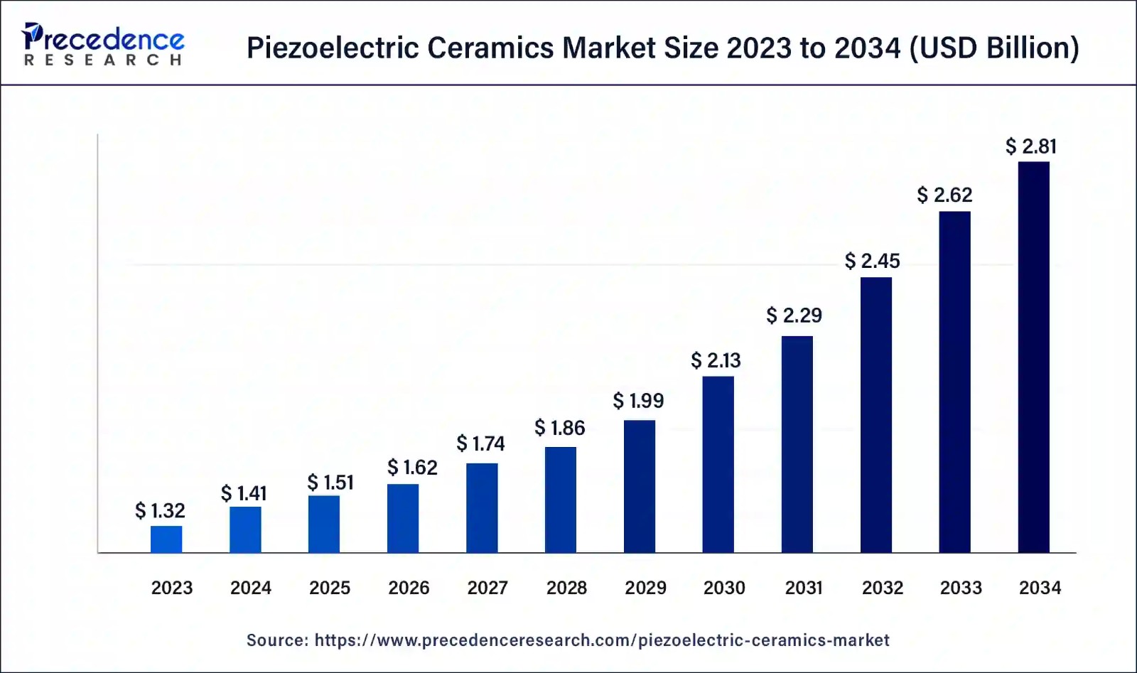
Fig. 1 Market Prospects of Piezoelectric MEMS Devices
SAW devices ultilize the characteristics of the acoustic waves propagating on the piezoelectric substrate surface to realize signal filtering and sensing. The related filters, delay lines, and sensors have been widely used in the fields of RF communications, environmental monitoring and so on. On this topic, our team mainly focus on the theoretical research, numerical research, optimization design and other scientific research.
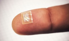
Fig. 2 SAW sensing unit[1]
Fig. 3 Finit element simulation of SAW on a piezoelectric substrate[2]
PMUTs use the mechanical vibration of piezoelectric film to transmit and receive ultrasound waves. They have shown great potentials in the fields of medical imaging (such as portable ultrasound probes), industrial non-destructive testing, consumer electronics (gesture recognition, distance sensing), and autonomous driving (close-range obstacle avoidance). Its miniaturization provide new possibilities for wearable devices and implantable medical devices. On this topic, our team mainly conduct research on numerical research, optimization design, and engineering applications.
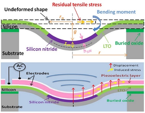
Fig. 4 Schematic diagram of PMUT device structure[3]
Research Interest 2: Optical MEMS Technology and Devices
With the rapid development of information technology and optical communication technology, a new area of MEMS is the combination of MEMS and optics, that is, to integrate basic technologies such as microelectronics, micromechanics, and optoelectronics for developing new optical devices, called micro-opto-electromechanical systems (optical MEMS). By this, various MEMS structural parts with micro-optical devices, optical waveguide devices, semiconductor laser devices, and photoelectric detection devices can be fully integrated. The achived devices can not only form new functional systems but also have the merits of small size, low cost, mass production, an so on. In this field, our team mainly focuses on MEMS micromirrors, especially on the related research of electrothermal MEMS micromirrors.
Compared with electrostatic, electromagnetic, and piezoelectric MEMS micromirrors, MEMS electrothermal micromirrors feature with low driving voltage and large deflection angle, which have become innovative solutions for advanced high-end application scenarios. Micro optical coherence tomography (OCT) endoscopic imagers, micro Fourier transform spectrometers (FTS), optical communications, and AR/VR displays, just to name a few. At present, our team is carrying out the related scientific research work including: optimization design, fabrication, drive control and peripheral circuit design. The corresponding achivements have been published as invention patents.
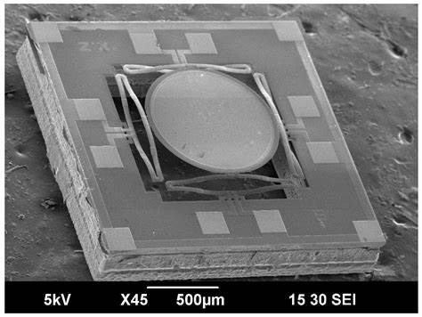
Fig. 5 MEMS electrothermal micromirror[4]
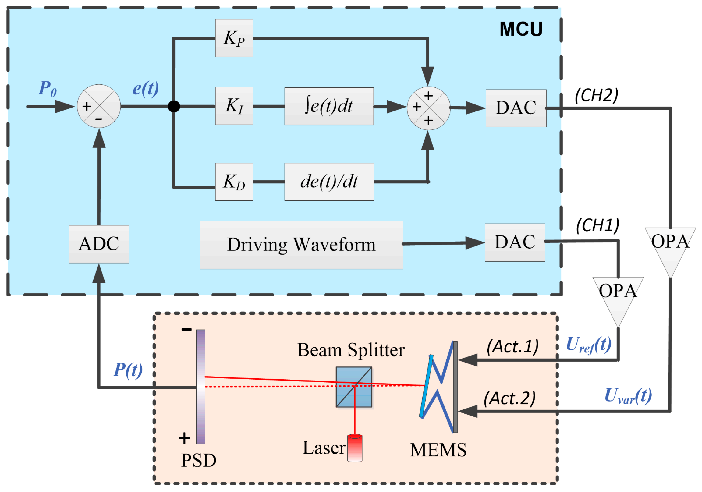
Fig. 6 The control circuit architecture of MEMS electrothermal micromirrors[5]
References
[1] https://www.transense.com/
[2] Collins D J, Devendran C, Ma Z, et al. Acoustic tweezers via sub–time-of-flight regime surface acoustic waves[J]. Science advances, 2016,2(7): e1600089.
[3] Soukup B H. Design of piezoelectric micromachined ultrasonic transducer (PMUT) arrays for intrabody networking applications[D]. Northeastern University, 2017.
[4] Zhou L, Zhang X, Xie H. An electrothermal Cu/W bimorph tip-tilt-piston MEMS mirror with high reliability[J]. Micromachines, 2019, 10(5): 323.
[5] Wang W, Chen J, Zivkovic A S, et al. A Fourier transform spectrometer based on an electrothermal MEMS mirror with improved linear scan range[J]. Sensors, 2016, 16(10): 1611.


